Figure 2 from Under Bump Metallurgy (UBM)-a technology review for flip chip packaging

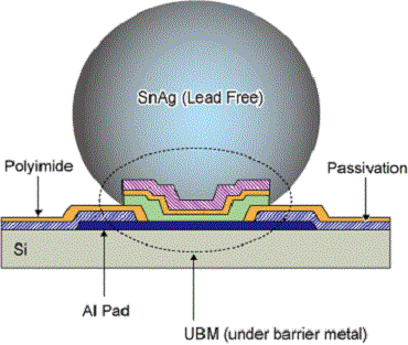
Fig. 2. Schematic cross-section of evaporated UBM and solder bump [12] - "Under Bump Metallurgy (UBM)-a technology review for flip chip packaging"

A study in flip-chip UBM/bump reliability with effects of SnPb

a) Schematic diagram of the flip‐chip package. b) Effects of

Figure 6 from Under Bump Metallurgy (UBM)-a technology review for
Artificial intelligence deep learning for 3D IC reliability prediction

A study in flip-chip UBM/bump reliability with effects of SnPb

Schematic of EM-aging test on flip-chip packages. Regions of void
Pb-Free Solders for Flip-Chip Interconnections
PDF) Investigation of under bump metallization systems for flip

PDF) Pb-free Sn/3.5Ag electroplating bumping process and under

Direct bump-on-copper process for flip chip technologies