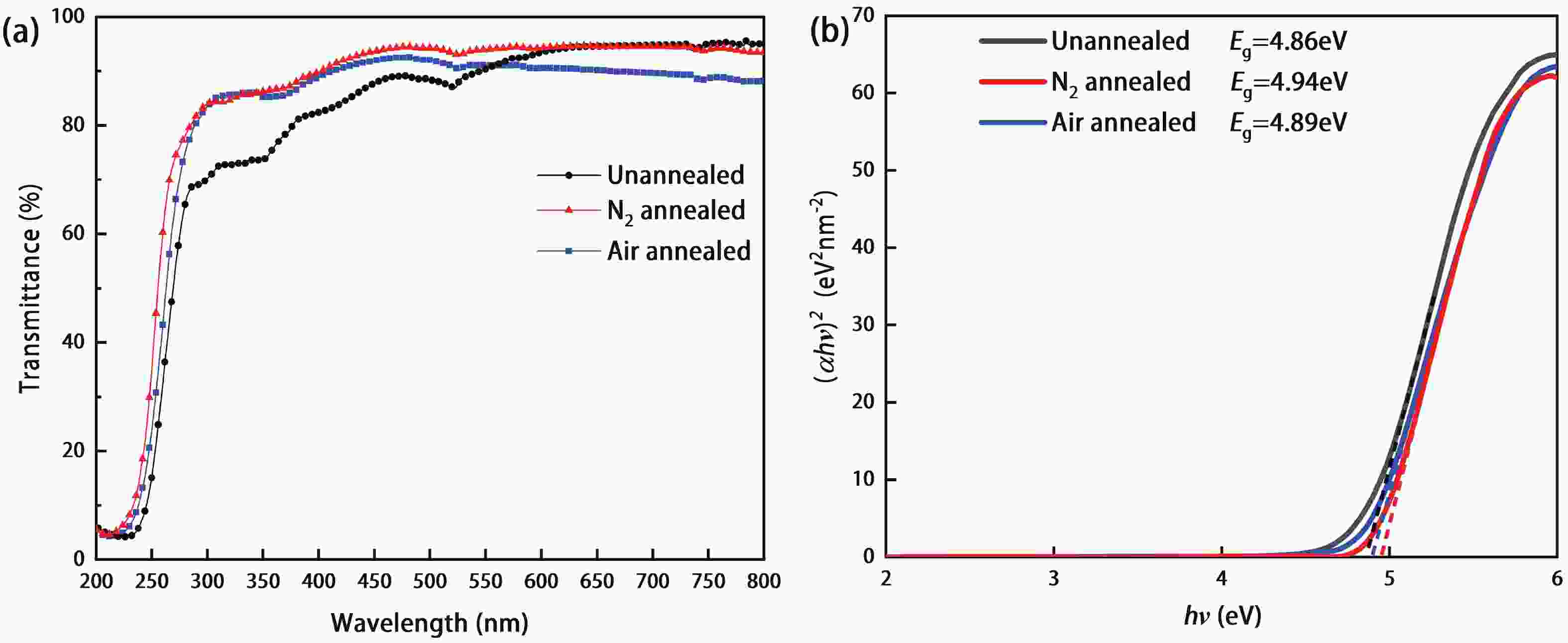
Deep UV transparent conductive oxide thin films realized through


Jiaye ZHANG, PhD Student, Doctor of Philosophy, Xiamen University, Xiamen, XMU, Chemical and Biochemical Engineering

Mobility and carrier concentration of Ga2O3:Si films from a Ga2O3-1 wt.

PDF) Computational Prediction and Experimental Realization of Earth-Abundant Transparent Conducting Oxide Ga-Doped ZnSb₂O

Energy diagram of an inverted OLED device using a-C12A7:e (EIL) and

Deep UV transparent conductive oxide thin films realized through degenerately doped wide-bandgap gallium oxide - ScienceDirect

David SCANLON, University College London, London, UCL, Department of Chemistry
Preparation of Sn-doped Ga2O3 thin films and their solar-blind photoelectric detection performance

Enhanced low-temperature response of Ga2O3-based oxygen sensor by modulating the surficial micro-nano structures - ScienceDirect

Conductivity of Ga2O3:Si thin films from Ga2O3 targets with different
Publications Chen Wei's Group
Issue: Cell Reports Physical Science

K. ZHANG, University of Oxford, Oxford, OX, Chemical Research Laboratory